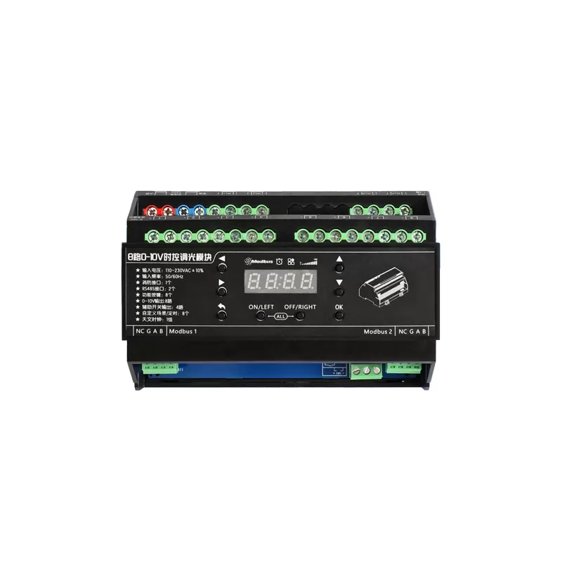
Communication Interface
- Communication Format:
- 1200, N, 8,1
- 2400, N, 8,1
- 4800, N, 8,1
- 9600, N, 8,1 (default)
- 19200, N, 8,1
- 38400, N, 8,1
- Slave Address:
- Address Range: 0x01-0x3F
- Address Setting: Physical Keys (see control panel operation)
- Protocol Format Description: Protocol verification supports fixed byte 0xAC 0xAC or CRC16 verification
Function code description
Function code 03H description
Host ->Slave sends: 01030002000265CB
Host<- Slave receives: 01030400FE 00415B F3
- Host ->Slave sends instruction definition:
- First byte 01H - Dimming device address (determined by device ID dialing)
- Second byte 03H - Modbus function code, reads the value of a single register or multiple registers
- 3rd and 4th bytes 0002H - Read the value of the register from the position of 0002H register
- 5th and 6th bytes 0002H - Starting from the registers specified in the 3rd and 4th bytes, read data from a total of 2 registers
- The 7th and 8th bytes 65CBH - are the checksum bytes (CRC16 high and low bits) for the frame data
- Host<- Slave receives instruction definition:
- The first byte 01H - Dimming device address (determined by dialing the device ID)
- The second byte is the 03H Modbus function code, which reads the value of a single register or multiple registers
- The third byte 04H - Dimming returns a total of 4 bytes of data
- 4th and 7th bytes 00020042H - Dimming returns a total of 4 bytes of data
- The 8th and 9th bytes 65CBH - are the checksum bytes (CRC16 high and low bits) for the frame data
Function code 06H description
Host ->Slave Send: 010600030041B9FA
Host<- Slave Receive: 010600030041B9FA
- Host ->Slave sends command definition:
- The first byte 01H - Dimming device address (determined by dialing the device ID)
- The second byte is the 06H Modbus function code, which writes the value of a single register
- The 3rd and 4th bytes 0003H - Write the register value starting from the 0003H register position
- 5th and 6th bytes 0041H - Write 0041H value from the registers specified in bytes 3,4
- The 7th and 8th bytes B9FAH - are the checksum bytes (CRC16 high and low bits) for the frame data
- Host<- Slave receives instruction definition:
- The first byte 01H - Dimming device address (determined by dialing the device ID)
- Second byte 06H - Modbus function code, write the value of a single register
- Third and fourth bytes 0003H - Write the value of the register from the position of 0003H
- Fifth and sixth bytes 0041H- Write 0041H value
- from the registers specified in bytes 3 and 4. The 7th and 8th bytes B9FAH - are the checksum bytes (CRC16 high and low bits) for the frame data
Function code 10H description
Host ->Slave Send: 01100001000204000100FE E223
Host<- Slave Receive: 0110000100021008
- Host ->Slave sends command definition:
- The first byte 01H - Dimming device address (determined by dialing the device ID)
- The second byte is the 10H Modbus function code, which writes the values of multiple registers at once
- The 3rd and 4th bytes 0001H - the value written to the register once starting from the position of the 0001H register
- 5th and 6th bytes 0002H - Starting from the register position specified in bytes 3 and 4, write the values of two registers at once
- Byte 7 04H - The total number of bytes to be written is 8 (2 registers * 2)
- Byte 8 and 9- The first register writes the value 0001H, and the second register writes the value 00FEH
- 10th and 11th bytes E223H - Check bytes (CRC16 high and low bits) for the frame data
- Host<- Slave instruction definition:
- 1st byte 01H - Dimming device address (determined by device ID dialing)
- 2nd byte 10H - Modbus function code, writing multiple register values at once
- 3rd and 4th bytes 0001H - Writing register values at once starting from the 0001H register position
- 5th and 6th bytes 0002H - Writing two register values at once starting from the specified register position in bytes 3,4
- 7th and 8th bytes 100H 8H - Check byte (CRC16 high and low bits) for this frame of data
Function code 01H Description
Host ->Slave sends: 0101000000083D CC
Host<- Slave receives: 010101FF 11C8
- Host ->Slave sends instruction definition:
- First byte 01H - Dimming device address (determined by device ID dialing)
- Second byte 01H - Modbus function code, reads the value of a single coil or multiple coils
- Third and fourth bytes 0000H - Read the value of a coil starting from the position of the 0000H coil
- Fifth and sixth bytes 0008H - Read data from 8 coils starting from the coil specified in the third and fourth bytes
- Seventh and eighth bytes 3DCCH - Check byte (CRC16 high and low bits) for this frame of data
- Host<- Slave instruction definition:
- 1st byte 01H - Dimming device address (determined by device ID dialing)
- 2nd byte 01H - Modbus function code, reads the value of a single coil or multiple coils
- 3rd byte 01H - Dimming returns a total of 1 byte of data length
- 4th byte FFH - Dimming returns 1 byte of data, coil bit: 1 on, 0 off, bit0 - bit7, Indicate that the 5th and 6th bytes 11C8H of
- are the checksum bytes (CRC16 high and low bits) for the frame data
I'm very sorry, it may have been due to an omission or formatting issue while organizing the content, which resulted in some parts being incomplete. Here are the complete instructions for function code 05H and function code 0FH to ensure information integrity:
Function code 05H description
Host ->Slave Send: 01050000FF 008C 3A
Host<- Slave Receive: 01050000FF 008C 3A
- Host ->Slave sends command definition:
- The first byte 01H - Dimming device address (determined by dialing the device ID)
- The second byte is the 05H Modbus function code, which writes the value of a single coil
- 3rd and 4th bytes 0000H - Write the value of the coil starting from the position of 0000H coil
- . The 5th and 6th bytes FF00H - write the FF00H value from the coil specified in bytes 3 and 4
- . The 7th and 8th bytes 8C3A - are the checksum bytes (CRC16 high and low bits) for the frame data
- Host<- Slave receive instruction definition:
- First byte 01H - Dimming device address (determined by device ID dialing)
- Second byte 05H - Modbus function code, write the value of a single coil
- 3rd and 4th bytes 0000H - Write the value of the coil starting from the position of 0000H coil
- 5th and 6th bytes FF00H - Write FF00H value from the coil specified in bytes 3 and 4
- Seventh and eighth bytes 8C3A - Check byte (CRC16 high and low bits) for this frame of data
Function code 0FH description
Host ->Slave sends: 010F 00000008010F BE 91
Master<- Slave receives: 010F 00000008540D
- Host ->Slave sends command definition:
- The first byte 01H - Dimming device address (determined by device ID dialing)
- The second byte 0FH Modbus function code, writing values for multiple coils at once
- The third and fourth bytes 0000H - Writing values for coils starting from the 0000H coil position
- The fifth and sixth bytes 0008H - Writing values for 8 coils at once starting from the coil position specified in the third and fourth bytes
- The seventh byte 01H - The total number of bytes to be written is 8 (2 registers * 2)
- The eighth byte 0FH - Writing values for the first register 000H 1H value, the second register writes 00FEH value
- The 9th and 10th bytes BE91H - are the checksum bytes (CRC16 high and low bits) of the frame data
- Host<- Slave receive instruction definition:
- The 1st byte 01H - Dimming device address (determined by device ID dialing)
- The 2nd byte 0FH Modbus Function code, write values for multiple coils at once
- 3rd and 4th bytes 0000H - write values for coils starting from the 0000H coil position
- 5th and 6th bytes 0008H - write values for 8 coils at once starting from the coil position specified in bytes 3,4
- The 7th and 8th bytes 540DH - are the check bytes (CRC16 high and low bits) of the frame data
. Next is a complete description of other function codes:
Function code 03H description
Host ->Slave send: 01030002000265CB
Host<- Slave receive: 01030400FE 00415B F3
- Host ->Slave send instruction definition:
- The 1st byte 01H - Dimming device address (determined by device ID dialing)
- The 2nd byte 03H Modbus function Code, read the value of a single register or multiple registers
- 3rd and 4th bytes 0002H - Read the value of the register from the position of the 0002H register
- 5th and 6th bytes 0002H - Read the data of 2 registers starting from the specified register in the 3rd and 4th bytes 0002H
- 7th and 8th bytes 65CBH - Check byte for the frame data (CRC16 high and low bits)
- Host<- Slave instruction definition:
- 1st byte 01H - Dimming device address (determined by device ID dialing)
- 2nd byte 03H - Modbus function code, reads the value of a single register or multiple registers
- 3rd byte 04H - Dimming returns 4 bytes of data
- 4th and 7th bytes 00020042H - Dimming returns 4 bytes of data
- 8th and 9th bytes 65CBH - Check byte (CRC16 high and low bits) for this frame of data
Function code 06H Description
Host ->Slave sends: 010600030041B9FA
Host<- Slave receives: 010600030041B9FA
- Host ->Slave sends instruction definition:
- First byte 01H - Dimming device address (determined by device ID dialing)
- Second byte 06H - Modbus function code, writing the value of a single register
- Third and fourth bytes 0003H - Writing the value of the register from the position of the 0003H register
- Fifth and sixth bytes 0041H - Writing the 0041H value from the register specified in the third and fourth bytes
- Seventh and eighth bytes B9FAH - Check byte (CRC16 high and low bits) for this frame of data
- Host -<- Slave receives instruction definition:
- The first byte 01H - Dimming device address (determined by dialing the device ID)
- The second byte 06H - Modbus function code, writing the value of a single register
- The third and fourth bytes 0003H - Writing the value of the register from the position of 0003H
- The fifth and sixth bytes 0041H- Write 0041H value
- from the registers specified in bytes 3 and 4. The 7th and 8th bytes B9FAH - are the checksum bytes (CRC16 high and low bits) for the frame data
Function Code 10H Description
Host ->Slave Sending: 01100001000204000100FE E223
Host -<Slave Receiving: 0110000100021008
- Host ->Slave Sending Instruction Definition:
- First Byte 01H - Dimming Device Address (determined by device ID dialing)
- Second Byte 10H - Modbus Function Code, writes multiple register values at once
- Third and Fourth Byte 0001H - Write register values starting from the position of 0001H
- Fifth and Sixth Byte Byte 0002H - Starting from the register position specified in bytes 3,4, write the values of two registers at once
- . Byte 04H - The total number of bytes to be written is 8 (2 registers * 2)
- . Byte 8,9- The first register writes the value 0001H, and the second register writes the value 00FEH
- 10th and 11th bytes E223H - Check bytes (CRC16 high and low bits) for the frame data
- Host<- Slave instruction definition:
- 1st byte 01H - Dimming device address (determined by device ID dialing)
- 2nd byte 10H - Modbus function code, writing values to multiple registers at once
- 3rd and 4th bytes 0001H - Writing values to registers at once starting from register position 0001H
- 5th and 6th bytes 0002H - Writing values to two registers at once starting from register position specified in bytes 3 and 4
- The 7th and 8th bytes 1008H - are the checksum bytes (CRC16 high and low bits) for the frame data
Function code 01H Description
Host ->Slave Sending: 010100000083D CC
Host<- Slave Receiving: 010101FF 11C8
- Host ->Slave sends instruction definition:
- First byte 01H - Dimming device address (determined by device ID dialing)
- Second byte 01H - Modbus function code, reads the value of a single coil or multiple coils
- Third and fourth bytes 0000H - Read the value of the coil from the position of the 0000H coil
- Fifth and sixth bytes 0008H - Read the data of 8 coils starting from the coil specified in the third and fourth bytes
- Seventh and eighth bytes 3DCCH - Check byte (CRC16 high and low bits) for this frame of data
- Host<- Slave instruction definition:
- 1st byte 01H - Dimming device address (determined by device ID dialing)
- 2nd byte 01H - Modbus function code, reads the value of a single coil or multiple coils
- 3rd byte 01H - Dimming returns a total of 1 byte of data length
- The 4th byte FFH - Dimming returns 1 byte of data, coil bit: 1 on, 0 off, bit0 - bit7, Indicate that the 5th and 6th bytes 11C8H of
- are the checksum bytes (CRC16 high and low bits) for the frame data
Function Code 05H Description
Host ->Slave Sending: 0105000FF 008C 3A
Host<- Slave Receiving: 0105000FF 008C 3A
- Host ->Slave Sending Instruction Definition:
- First Byte 01H - Dimming Device Address (determined by device ID dialing)
- Second Byte 05H - Modbus Function Code, Writing the Value of a Single Coil
- Third and Fourth Byte 0000H - Writing the Value of a Coil Starting from the Position of 0000H
- 5th and 6th bytes FF00H - Write FF00H value from the coil specified in bytes 3 and 4
- The 7th and 8th bytes 8C3A - are the checksum bytes (CRC16 high and low bits) for the frame data
- Host<- Slave receives instruction definition:
- The first byte 01H - Dimming device address (determined by dialing the device ID)
- The second byte is the 05H Modbus function code, which writes the value of a single coil
- 3rd and 4th bytes 0000H - Write the value of the coil starting from the position of 0000H coil
- 5th and 6th bytes FF00H - Write FF00H value from the coil specified in bytes 3 and 4
- The 7th and 8th bytes 8C3A - are the checksum bytes (CRC16 high and low bits) for the frame data
Function code 0FH description
Host ->Slave Send: 010F 00000008010F BE 91
Host<- Slave Receive: 010F 00000008540D
- Host ->Slave Send Instruction Definition:
- First Byte 01H - Dimming Device Address (determined by device ID dialing)
- 2nd byte 0FH Modbus function code, write values for multiple coils at once
- The 3rd and 4th bytes 0000H - Write the values of the coils in sequence starting from the coil position 0000H
- 5th and 6th bytes 0008H - Starting from the coil position specified in bytes 3 and 4, write the values of 8 coils at once
- The 7th byte 01H - The total number of bytes to be written is 8 (2 registers * 2)
- The 8th byte 0FH - the 1st register writes the value 0001H, and the 2nd register writes the value 00FEH
- The 9th and 10th bytes BE91H - are the checksum bytes (CRC16 high and low bits) for the frame data
- Host<- Slave receives instruction definition:
- The first byte 01H - Dimming device address (determined by dialing the device ID)
- 2nd byte 0FH Modbus function code, write values for multiple coils at once
- The 3rd and 4th bytes 0000H - Write the values of the coils in sequence starting from the coil position 0000H
- 5th and 6th bytes 0008H - Starting from the coil position specified in bytes 3 and 4, write the values of 8 coils at once
- The 7th and 8th bytes 540DH - are the checksum bytes (CRC16 high and low bits) for the frame data
I'm very sorry for the inconvenience caused to you. The following is the complete register address table content:
Register Address Table
1. Simplified Register Address Table
| Function | Register Dec | Register Hex | Register data Hex | Read/Write | Function code Hex |
|---|---|---|---|---|---|
| Dimming circuit 1-8 | 1-8 | 0000H-0007H | High position: 00 Low level: 00-64 (brightness 0-100) | R/W | 03/06/10 |
| Scene configuration register | 64-127 | 0040H-007FH | High position: 00 Low level: 00-64 (dimming brightness 0-100) | R/W | 03/06/10 |
| Gradient time register | 128-135 | 0080H-0087H | High position: 00 Low level: 00-64 (gradient time, unit: s) | R/W | 03/06/10 |
| Power on brightness register | 136-143 | 0088H-008FH | High position: 00 Low level: 00 (closed) 01-64 (Enable 1-100%) FF (Recovery) | R/W | 03/06/10 |
| Brightness minimum value register | 144-151 | 0090H-0097H | High position: 00 Low level: 00-14 (minimum brightness output value 0-2V) | R/W | 03/06/10 |
| Brightness maximum value register | 152-159 | 0098H-009FH | High position: 00 Low level: 50-64 (maximum brightness output of 8-10V) | R/W | 03/06/10 |
| Time and date setting register | 184-190 | 00B8H-00BEH | Year: 0000-0063 (0-99) Month: 0001-000C (1-12) Date: 0001-001F (1-31) Time: 0000-0017 (0-23) Score: 0000-003B (0-59) Seconds: 0000-003B (0-59) Week: 0001-0007 (read-only) | R/W | 03/06/10 |
| Scene call register | 191 | 00BFH | High position: 00 Low level: 01-08 (Scenario 1-8) | W | 06 |
| Baud rate setting register (RS485 left) | 192 | 00C0H | High position: 00 Low level: 0000 (1200) 0001 (2400) 0002 (4800) 0003 (9600, Default: 0004 (19200) 0005 (38400) | R/W | 03/06 |
| Baud Rate Setting Register (RS485 Right) | 193 | 00C1H | High Bit: 00 Low Bit: 0000 (1200) 0001 (2400) 0002 (4800) 0003 (9600, default) 0004 (19200) 0005 (38400) | R/W | 03/06 |
| Factory register | 194 | 00C2H | High position: 00 Low level: 01 (device restored to factory state) | W | 06 |
| Version Register | 195-197 | 00C3H-00C5H | Year: 2025 dec ->07E9H Month Day: 0519dec ->0207H Version: 0100dec ->0064H | R | 03 |
| Weekly timer setting register | 216-311 | 00D8H-0137H | Switch: 0000 (off) 0001 (enabled) Hour: 0000-0017 (0-23) Minutes: 0000-003B (0-59) Week: 0000-007F (Monday: bit0, Tuesday: bit1,..., Sunday: bit6, bit7:0) Circuit 1-8 status: 0000-0064 (dimming value) 00FF (not executed) | R/W | 03/06/10 |
| Sunrise and Sunset Setting Register | 320-349 | 0140H-015DH | Longitude: High Altitude 00 Low position 00/01 (East/West longitude) Degree: High level 00 Low level 0-180 Score: High 00 Low level 0-59 Latitude: High Altitude 00 Low position 00/01 (North/South latitude) Degree: High level 00 Low level 0-180 Score: High 00 Low level 0-59 Sunrise Time: Hour 0000-0017 Minutes 0000-003B Sunset time: hours 0000-0017 Minutes 0000-003B Sunrise timer: switch 0000 (off) 0001 (enabled) Week 0000-007F Circuit 1-8 status: 0000-0064 (dimming value) 00FF (not executed) Sunset timing: Same as sunrise timing | R/W | 03/06/10 |
| Auxiliary register | 2001-2064 | 07D1H-0810H | Please refer to the auxiliary register address table for details | W | 10 |
2. Loop control register address
| Function | Loop 1 Register | Loop 2 Register | Loop 3 Register | Loop 4 Register | Loop 5 Register | Loop 6 Register | Loop 7 Register | Loop 8 register |
|---|---|---|---|---|---|---|---|---|
| Circuit 1-8 | 0000H | 0001H | 0002H | 0003H | 0004H | 0005H | 0006H | 0007H |
3. Scene setting register address
I apologize to you, there was indeed an error. Let me reorganize and provide the remaining part of the scene settings register address in its entirety.
Scene Setting Register Address (Continued)
Continuing with the scenario above, set the register address table:
| Function | Loop 1 Register | Loop 2 Register | Loop 3 Register | Loop 4 Register | Loop 5 Register | Loop 6 Register | Loop 7 Register | Loop 8 register |
|---|---|---|---|---|---|---|---|---|
| Scenario 1 | 0040H | 0041H | 0042H | 0043H | 0044H | 0045H | 0046H | 0047H |
| Scene 2 | 0048H | 0049H | 004AH | 004BH | 004CH | 004DH | 004EH | 004FH |
| Scenario 3 | 0050H | 0051H | 0052H | 0053H | 0054H | 0055H | 0056H | 0057H |
| Scene 4 | 0058H | 0059H | 005AH | 005BH | 005CH | 005DH | 005EH | 005FH |
| Scene 5 | 0060H | 0061H | 0062H | 0063H | 0064H | 0065H | 0066H | 0067H |
| Scenario 6 | 0068H | 0069H | 006AH | 006BH | 006CH | 006DH | 006EH | 006FH |
| Scenario 7 | 0070H | 0071H | 0072H | 0073H | 0074H | 0075H | 0076H | 0077H |
| Scenario 8 | 0078H | 0079H | 007AH | 007BH | 007CH | 007DH | 007EH | 007FH |
These addresses are used to configure and call different scenes, and each scene can set brightness values for 8 circuits (channels). The brightness value range of each circuit is 0-100%, which is set by writing data to the corresponding register.
Of course, I will continue to provide the remaining register address table information in the document:
4. Gradient time register address
| Function | Loop 1 Register | Loop 2 Register | Loop 3 Register | Loop 4 Register | Loop 5 Register | Loop 6 Register | Loop 7 Register | Loop 8 register |
|---|---|---|---|---|---|---|---|---|
| Transition time of loop 1-8 | 0080H | 0081H | 0082H | 0083H | 0084H | 0085H | 0086H | 0087H |
5. Power on brightness register address
| function | loop 1 register | loop 2 register | loop 3 register | Loop 4 Register | Loop 5 Register | Loop 6 Register | Loop 7 Register | Loop 8 Register |
|---|---|---|---|---|---|---|---|---|
| Loop 1-8 Power on Brightness | 0088H | 0089H | 008AH | 008BH | 008CH | 008DH | 008EH | 008FH |
6. Address of the minimum brightness value register
| Function | Loop 1 Register | Loop 2 Register | Loop 3 Register | Loop 4 Register | Loop 5 Register | Loop 6 Register | Loop 7 Register | Loop 8 register |
|---|---|---|---|---|---|---|---|---|
| Minimum Brightness Values for Circuits 1-8 | 0090H | 0091H | 0092H | 0093H | 0094H | 0095H | 0096H | 0097H |
7. Address of the maximum brightness value register
| Function | Loop 1 Register | Loop 2 Register | Loop 3 Register | Loop 4 Register | Loop 5 Register | Loop 6 Register | Loop 7 Register | Loop 8 Register |
|---|---|---|---|---|---|---|---|---|
| Loop 1-8 Brightness Maximum | 0098H | 0099H | 009AH | 009BH | 009CH | 009DH | 009EH | 009FH |
8. Time and Date Setting Register Address
| Function | Year Register | Month Register | Day Register | Hour Register | Minute Register | Second Register | Week Register |
|---|---|---|---|---|---|---|---|
| Time and Date | 00B8H | 00B9H | 00BAH | 00BBH | 00BCH | 00BDH | 00BEH |
9. Week Timer Setting Register Address
| Function | Timer 1 | Timer 2 | Timer 3 | Timer 4 | Timer 5 | Timer 6 | Timer 7 | Timer 8 |
|---|---|---|---|---|---|---|---|---|
| Timer Switch | 00D8H | 00E4H | 00F0H | 00FCH | 0108H | 0114H | 0120H | 012CH |
| Timer hours | 00D9H | 00E5H | 00F1H | 00FDH | 0109H | 0115H | 0121H | 012DH |
| Timer minutes | 00DAH | 00E6H | 00F2H | 00FEH | 010AH | 0116H | 0122H | 012EH |
| Timer Week | 00DBH | 00E7H | 00F3H | 00FFH | 010BH | 0117H | 0123H | 012FH |
10. Setting register address for sunrise and sunset
| Function | Sunrise timing | Sunset timer |
|---|---|---|
| switch | 014AH | 0154H |
| Week | 014BH | 0155H |
| Loop 1-8 Status | 014CH-0151H | 0156H-0161H |
11. Auxiliary Register Address
| Loop | Gradient Time Register | Brightness Register | Reserve Register 1 | Reserve Register 2 | Reserve Register 3 | Reserve Register 4 | Reserve Register 5 | Reserve Register 6 | Reserve Register 7 | Reserve Register 8 |
|---|---|---|---|---|---|---|---|---|---|---|
| 3 | 07E1H | 07E2H | 07E3H | 07E4H | 07E5H | 07E6H | 07E7H | 07E8H | ||
| 4 | 07E9H | 07EAH | 07EBH | 07ECH | 07EDH | 07EEH | 07EFH | 07F0H | ||
| 5 | 07F1H | 07F2H | 07F3H | 07F4H | 07F5H | 07F6H | 07F7H | 07F8H | ||
| 6 | 07F9H | 07FAH | 07FBH | 07FCH | 07FDH | 07FEH | 07FFH | 0800H | ||
| 7 | 0801H | 0802H | 0803H | 0804H | 0805H | 0806H | 0807H | 0808H | ||
| 8 | 0809H | 080AH | 080BH | 080CH | 080DH | 080EH | 080FH | 0810H |
These auxiliary registers provide additional flexibility, allowing users to store and manipulate more custom data. For example, gradient time registers and brightness registers can be used to control the gradient effect and brightness level of lights, while reserved registers provide space for future functional extensions or specific applications. The
protocol routines
document also provides some protocol routines that demonstrate how to communicate with the dimming module using the Modbus protocol. Here are some examples:
- Writing Single Channel Switch Instruction Register (05H Function Code)
- Instruction:
01 05 00 00 FF 00 8C 3A - Feedback:
01 05 00 00 FF 00 8C 3A - Comment: Loop 1 is turned on
- Write single dimming instruction register (06H function code)
- Instruction:
01 06 00 00 00 64 88 21 - Feedback:
01 06 00 00 00 64 88 21 - Comment: Loop 1 brightness is adjusted to 100%
- Write multi way switch instruction register (0FH function code)
- Instruction:
01 0F 00 00 00 08 01 FF BE D5 - Feedback:
01 0F 00 00 00 08 54 0D - Comment: Loop 1-8 is turned on
- Write multi way dimming instruction register (10H function code)
- Instruction:
01 10 00 00 08 10 64 00 64 00 64 00 64 00 64 00 64 00 64 97 0B - Feedback:
01 10 00 00 08 C1 CF - Comment: Adjust the brightness of loop 1-8 to 100%
Continue to provide detailed information about the protocol routine in the document:
- Read switch status instruction register (01H function code)
- Instruction:
01 01 00 00 00 08 3D CC - Feedback:
01 01 01 FF 11 C8 - Comment: Read 1-8 channels, turn on loop 1-8
- Read dimming status instruction register (03H function code)
- Instruction:
01 03 00 00 00 01 84 0A - Feedback:
01 03 02 00 64 B9 AF - Comment: Read single channel, loop 1 brightness 100%
- Write Single channel Dimming Gradient Time Instruction Register (06H Function Code)
- Instruction:
01 06 00 80 00 03 C8 23 - Feedback:
01 06 00 80 00 03 C8 23 - Comment: Loop 1 Gradient Time 3s
- Write Multi channel Dimming Gradient Time Instruction Register (10H Function Code)
- Instruction:
01 10 00 80 08 10 03 03 03 03 03 03 03 03 03 03 03 9C 64 - Feedback:
01 10 00 80 08 C0 27 - Comment: Loop 1-8 Gradient Time 5s
- Call Scene Instruction Register (06H Function Code)
- Instruction:
01 06 00 BF 00 01 79 EE - Feedback:
01 06 00 BF 00 01 79 EE - Comment: Call Scene 1
- Scene Configuration Instruction Register (10H Function Code)
- Instruction:
01 10 00 40 08 10 64 00 64 00 64 00 64 00 64 00 64 00 64 99 C4 - Feedback:
01 10 00 40 08 C0 1B - Comment: Configure Scene 1 status, Circuit 1-8 open
- Instruction:
- Power on Status Instruction Register (10H Function Code)
- Instruction:
01 10 00 88 08 10 FF 00 FF 00 FF 00 FF 00 FF 00 FF 00 FF 11 6C - Feedback:
01 10 00 88 08 41 E5 - Comment: Circuit 1-8 power on status is power-off recovery
- Instruction:
- Time and date Read/Write Instruction Register (03H/10H Function Code)
- Instruction:
01 10 00 B8 06 0C 00 19 00 06 00 03 00 D0 00 32 00 09 65 - Feedback:
01 10 00 B8 06 C0 2E - Comment: Set June 3, 2025 at 13:45
- Instruction:
- Sunrise and Sunset Timer Setting Instruction Register (10H Register)
- Instruction:
01 10 14 A0 0A 14 00 01 00 7F 00 00 00 00 00 00 00 00 00 00 65 84 - Feedback:
01 10 14 A0 0A 60 24 - Comment: Enable sunrise timer, executed daily, loop 1-8, brightness execution 0%
- Instruction:
- Week Timer Setting Instruction Register (03/10H Function Code)
- Instruction:
01 10 00 D8 0C 18 00 01 00 08 00 00 1F 00 00 00 00 00 00 00 00 00 16 3C - Feedback:
01 10 00 D8 0C 40 37 - Comment: Enable timer 1, executed at 8:00 am from Monday to Friday, loop 1-8 brightness execution 0%
- Instruction:
- Restore factory settings instruction register (06 Function Code)
- Instruction:
01 06 00 C2 00 01 E9 F6 - Feedback:
01 06 00 C2 00 01 E9 F6 - Comment: All device parameters Restore factory state
- Instruction:
- Baud rate setting instruction register (03H/06H function code)
- Instructions:
01 06 00 C0 00 03 C9 F7 - Feedback:
01 06 00 C0 00 03 C9 F7 - Note: The baud rate of the left serial port is set to 9600
- Instructions:
- Device version reading instruction register (03 function code)
- Instructions:
01 03 00 C3 00 03 F5 F7 - Feedback:
01 03 06 07 E9 02 07 06 4C C8 - Comment: The current version is: 20250519V1.0
- Instructions:
Okay, I will continue to provide the remaining protocol routine information in the document:
Protocol Routine (Continued)
- Call the scene instruction register (06H function code)
- Instructions:
01 06 00 BF 00 02 39 EF - Feedback:
0106 00BF 0002 39 EF - Comment: Call Scenario 2
- Call the scene instruction register (06H function code)
- Instructions:
01 06 00 BF 00 03 F8 2F - Feedback:
010600 BF00 03 F8 2F - Comment: Call Scenario 3
- Call the scene instruction register (06H function code)
- Instructions:
01 06 00 BF 00 04 B9 ED - Feedback:
01 06 00 BF 00 04 B9 ED - Comment: Call Scenario 4
- Call the scene instruction register (06H function code)
- Instructions:
01 06 00 BF 00 05 78 2D - Feedback:
0106 00 BF 00 05 78 2D - Comment: Call Scenario 5
- Call the scene instruction register (06H function code)
- Instructions:
010600BF0006382C - Feedback:
010600BF0006382C - Comment: Call Scenario 6
- Call the scene instruction register (06H function code)
- Instructions:
010600BF00 07F9 EC - Feedback:
010600 BF0007F9 EC - Comment: Call Scenario 7
- Call the scene instruction register (06H function code)
- Instructions:
010600BF0008B9E8 - Feedback:
010600 BF0008 B9 E8 - Comment: Call Scenario 8
- Scene configuration instruction register (10H function code)
- Instructions:
0110004000.081000.6400.640064.00 6400 64 00 64 00 64 00 64 99 C4 - Feedback:
011000400008C01B - Comment: Configure Scenario 1 status, Circuit 1-8 open
- Scene configuration instruction register (10H function code)
- Instructions:
0110004800081000000000000 000000000000000000F64B - Feedback:
01100048000841D9 - Comment: Configure Scenario 2 status, Circuit 1-8 off
- Power on status instruction register (10H function code)
- Instructions:
011000 8800081000FF00 FF00 FF00 FF 00 FF 00 FF 00 FF 00 FF 11 6C - Feedback:
01100088000841 E5 - Note: The power on status of circuit 1-8 is power off and restored
- Power on status instruction register (10H function code)
- Instructions:
0110008800081000000000000 000000000000000000E75A - Feedback:
01100088000841E5 - Note: The power on status of circuit 1-8 is closed
- Power on status instruction register (10H function code)
- Instructions:
0110008800081000640064006400 640064006400640064699C - Feedback:
01100088000841E5 - Note: The power on status of circuits 1-8 is 100%
- Time and date read/write instruction register (03H/10H function code)
- Instructions:
010300B80007842D - Feedback:
01030E001900060003000D 003800090002EAF2 - Note: The current time is: June 3, 2025, 13:26:9, Tuesday
These protocol routines cover various operations of the dimming module, including scene calling, scene configuration, power on state setting, and reading and writing of time and date. These operations are implemented through the Modbus RTU protocol, allowing users to control and monitor the status of the dimming module by sending specific instructions.
Continue to provide the remaining protocol routine information in the document:
- Sunrise and Sunset Timer Setting Instruction Register (10H Function Code)
- Instructions:
01 10 01 4A 00 0A 14 00 01 00 7F 00 00 00 00 00 00 00 00 00 65 84 - Feedback:
01 10 01 4A 00 0A 60 24 - Note: Enable sunrise timer, execute daily, loop 1-8, brightness execution 0%
- Sunrise and Sunset Timer Setting Instruction Register (10H Function Code)
- Instructions:
01 10 01 54 00 0A 14 00 01 6400 64 00 64 00 64 00 64 00 64 00 64 82 - Feedback:
01 10 01 54 00 0A 00 22 - Note: Enable sunset timer, executed daily, circuits 1-8, brightness executed 100%
- Read Sunrise Status Instruction Register (10H Function Code)
- Instruction:
01 03 01 4A 00 0A E5 E7 - Feedback:
01 03 14 00 01 00 7F 00 00 00 00 00 00 00 00 00 00 00 8E B3 - Comment: Read Sunrise Status, Enable Sunrise Timing, Execute Every Day, Loop 1-8, Brightness Execution 0%
- Read Sunset Status Instruction Register (10H Function Code)
- Instruction:
01 03 01 54 00 0A 85 E1 - Feedback:
01 03 14 00 01 7F 00 64 00 64 00 64 00 64 00 64 00 64 75 - Comment: Read Sunset Status, Enable Sunset Timing, Execute Every Day, Loop 1-8, Brightness Execution 100%
- Weekly Timing Setting Instruction Register (03/10H Function Code)
- Instruction:
01 10 00 D8 00 0C 18 00 01 00 08 00 00 1F 00 00 00 00 00 00 00 00 00 16 3C - Feedback:
01 10 00 D8 00 0C 40 37 - Comment: Activate Timer 1, execute at 8:00 am from Monday to Friday, with 0% brightness execution for circuits 1-8
- Weekly timed instruction register (03/10H function code)
- Instructions:
01 10 00 E4 00 0C 18 00 01 00 12 00 00 1F 6400 64 00 64 00 64 00 64 4C C1 - Feedback:
01 10 00 E4 00 0C 80 3B - Note: Activate Timer 2, run from Monday to Friday at 18:00 pm, with brightness running at 100% for circuits 1-8
- Read the status instruction register of timer 1 (03/10H function code)
- Instructions:
01 03 00 D8 00 0C C5 F4 - Feedback:
01 03 18 00 01 00 08 00 00 1F 00 00 00 00 00 00 00 00 00 10 16 - Comment: Read the status of timer 1, enable timer, execute at 8:00 am from Monday to Friday, and execute 0% brightness for circuits 1-8
- Read the status instruction register of timer 2 (03/10H function code)
- Instructions:
01 03 00 E4 00 0C 05 F8 - Feedback:
01 03 18 00 01 00 12 00 00 1F 00 64 00 64 00 64 00 64 00 64 26 EB - Comment: Read the status of timer 2, enable timer, execute at 18:00 from Monday to Friday, and execute 100% brightness for circuits 1-8
- Factory Reset Instruction Register (06 Function Code)
- Instruction:
01 06 00 C2 00 01 E9 F6 - Feedback:
01 06 00 C2 00 01 E9 F6 - Comment: All device parameters are restored to factory state
- Baud Rate Setting Instruction Register (03H/06H Function Code)
- Instruction:
01 06 00 C0 00 03 C9 F7 - Feedback:
01 06 00 C0 00 03 C9 F7 - Comment: Left serial port baud rate set to 9600
- Baud Rate Setting Instruction Register (03H/06H Function Code)
- Instruction:
01 06 00 C1 00 05 51 35 - Feedback:
01 06 00 C1 00 05 51 35 - Comment: Right serial port baud rate set to 38400
- Read the current baud rate instruction register (03H function code) of the left serial port
- Instructions:
01 03 00 C0 00 01 84 36 - Feedback:
01 03 02 00 03 F8 45 - Note: The current baud rate of the left serial port is 9600
- Read the current baud rate instruction register (03H function code) of the right serial port
- Instructions:
01 03 00 C1 00 01 D5 F6 - Feedback:
01 03 02 00 05 78 47 - Note: The current baud rate of the right serial port is 38400
- Device version reading instruction register (03 function code)
- Instructions:
01 03 00 C3 00 03 F5 F7 - Feedback:
01 03 06 07 E9 02 07 06 4C C8 - Comment: The current version is: 20250519V1.0
These protocol routines provide detailed instructions and feedback information to help users understand and communicate with dimming modules using the Modbus protocol. If you have any questions or need further assistance, please feel free to let me know.
32.Baud rate setting instruction register (06H function code)
- Instructions:
010600C10005 518357 - Feedback:
010600C10005 518357 - Note: The baud rate of the right serial port is set to 38400
33.Device version reading instruction register (03 function code)
- Instructions:
010300C30003F5F7 - Feedback:
0103060702E902070064CC87
The above is a complete list of protocol routines provided in the document. These routines demonstrate how to communicate with 8-channel 0-10V dimming modules through Modbus RTU protocol, including setting and reading various parameters such as scene configuration, time and date, sunrise and sunset timing, week timing, baud rate setting, and device version information.
I noticed that the screenshot you provided contains specific information about the scene setting register address, which may be something you need to know. The following is the detailed information of setting register addresses based on the screenshot content:
Scene Setting Register Address
Scene 1
- Loop 1 Register: 0040H
- Loop 2 Register: 0041H
- Loop 3 Register: 0042H
- Loop 4 Register: 0043H
- Loop 5 Register: 0044H
- Loop 6 Register: 0045H
- Loop 7 Register: 0046H
- Loop 8 Register: 0047H
Scene 2
- Loop 1 Register: 0048H
- Loop 2 Register: 0049H
- Loop 3 Register: 004AH
- Loop 4 Register: 004BH
- Loop 5 Register: 004CH
- Loop 6 Register: 004DH
- Circuit 7 Register: 004EH
- Loop 8 Register: 004FH
Scenario 3
- Loop 1 Register: 0050H
- Loop 2 Register: 0051H
- Loop 3 Register: 0052H
- Loop 4 Register: 0053H
- Loop 5 Register: 0054H
- Loop 6 Register: 0055H
- Loop 7 Register: 0056H
- Loop 8 Register: 0057H
These addresses are used to set and call different scenes, and each scene can be configured with brightness values for 8 circuits (channels). By writing data to the corresponding registers, precise control of light brightness can be achieved.
Based on the screenshot you provided, I will continue to supplement and improve the detailed information of the scene setting register address:
Scene Setting Register Address (Continued)
Scenario 4
- Loop 1 Register: 0058H
- Loop 2 Register: 0059H
- Loop 3 Register: 005AH
- Loop 4 Register: 005BH
- Loop 5 Register: 005CH
- Loop 6 Register: 005DH
- Loop 7 Register: 005EH
- Loop 8 Register: 005FH
Scenario 5
- Loop 1 Register: 0060H
- Loop 2 Register: 0061H
- Loop 3 Register: 0062H
- Loop 4 Register: 0063H
- Loop 5 Register: 0064H
- Loop 6 Register: 0065H
- Loop 7 Register: 0066H
- Loop 8 Register: 0067H
Scenario 6
- Loop 1 Register: 0068H
- Loop 2 Register: 0069H
- Loop 3 Register: 006AH
- Loop 4 Register: 006BH
- Loop 5 Register: 006CH
- Loop 6 Register: 006DH
- Loop 7 Register: 006EH
- Loop 8 Register: 006FH
Scenario 7
- Loop 1 Register: 0070H
- Loop 2 Register: 0071H
- Loop 3 Register: 0072H
- Loop 4 Register: 0073H
- Loop 5 Register: 0074H
- Loop 6 Register: 0075H
- Loop 7 Register: 0076H
- Loop 8 Register: 0077H
Scenario 8
- Loop 1 Register: 0078H
- Loop 2 Register: 0079H
- Loop 3 Register: 007AH
- Circuit 4 Register: 007BH
- Loop 5 Register: 007CH
- Loop 6 Register: 007DH
- Circuit 7 Register: 007EH
- Loop 8 Register: 007FH
These register addresses allow users to configure different brightness levels for each circuit, creating multiple lighting scenarios. Through the Modbus protocol, users can write data to these registers to set or modify scene configurations.
Use scenario configuration instruction register (10H function code)
For example, to configure the state of scenario 1 to enable all circuits 1-8, the following command can be used:
- Instructions:
01100040000810006400640064 006400640064 006400640064 006400640064 99C4 - Feedback:
011000400008C01B
This instruction uses a 10H function code to write multiple register values at once. In this example, it sets the brightness value of all circuits (1-8) in scene 1 to 100% (64H).
Based on the screenshot you provided, I will continue to supplement and improve the detailed information of the scene setting register address:
Scene Setting Register Address (Continued)
Scenario 4
- Loop 1 Register: 0058H
- Loop 2 Register: 0059H
- Loop 3 Register: 005AH
- Loop 4 Register: 005BH
- Loop 5 Register: 005CH
- Loop 6 Register: 005DH
- Loop 7 Register: 005EH
- Loop 8 Register: 005FH
Scene 5
- Loop 1 Register: 0060H
- Loop 2 Register: 0061H
- Circuit 3 Register: 0062H
- Circuit 4 Register: 0063H
- Loop 5 Register: 0064H
- Loop 6 Register: 0065H
- Circuit 7 Register: 0066H
- Loop 8 Register: 0067H
Scenario 6
- Loop 1 Register: 0068H
- Loop 2 Register: 0069H
- Circuit 3 Register: 006AH
- Circuit 4 Register: 006BH
- Loop 5 Register: 006CH
- Loop 6 Register: 006DH
- Circuit 7 Register: 006EH
- Loop 8 Register: 006FH
Scenario 7
- Loop 1 Register: 0070H
- Loop 2 Register: 0071H
- Loop 3 Register: 0072H
- Loop 4 Register: 0073H
- Loop 5 Register: 0074H
- Loop 6 Register: 0075H
- Loop 7 Register: 0076H
- Loop 8 Register: 0077H
Scenario 8
- Loop 1 Register: 0078H
- Loop 2 Register: 0079H
- Loop 3 Register: 007AH
- Circuit 4 Register: 007BH
- Loop 5 Register: 007CH
- Loop 6 Register: 007DH
- Circuit 7 Register: 007EH
- Loop 8 Register: 007FH
These register addresses allow users to configure different brightness levels for each circuit, creating multiple lighting scenarios. Through the Modbus protocol, users can write data to these registers to set or modify scene configurations.
Use scenario configuration instruction register (10H function code)
For example, to configure the state of scenario 1 to enable all circuits 1-8, the following command can be used:
- Instructions:
01100040000810006400640064 006400640064 006400640064 006400640064 99C4 - Feedback:
011000400008C01B
This instruction uses a 10H function code to write multiple register values at once. In this example, it sets the brightness value of all circuits (1-8) in scene 1 to 100% (64H).
Protocol routine
- Restore factory settings command register (06 function code)
- Instructions:
010600C20001E9 F6 - Feedback:
010600C20001E9F6 - Comment: All device parameters are restored to factory state
- Instructions:
- Baud rate setting instruction register (03H/06H function code)
- Instruction:
01 06 00 C0 00 03 C9 F7 - Feedback:
010600C00003C9 F7 - Comment: Left serial port baud rate is set to 9600
- Instruction:
010600C1000518357 - Feedback:
010600C1000518357 - Comment: Set the baud rate of the right serial port to 38400
- Instructions:
01 03 00 C0 00 01 84 36 - Feedback:
0103020003F845 - Comment: The current baud rate of the left serial port is 9600
- Instruction:
01 03 00 C1 00 01 D5 F6 - Feedback:
01030200057847 - Comment: The current baud rate of the right serial port is 38400
- Instruction:
- Device version read instruction register (03 function code)
- Instruction:
010300C30003F5F7 - Feedback:
01030607E902070064CC87 - Comment: The current version is 20250519V1.0
- Instruction:
Of course, the following is the extracted content at the end of the document:
VI. Control Panel
1. Key Functions
| Icon | Meaning | Remarks |
|---|---|---|
| Left Button | ||
| Right Button | ||
| Up Button | ||
| Down Button | ||
| Return | ||
| ON/LEFT | Full Open/Left Move | |
| OFF/RIGHT | Full Key/Right Move | |
| OK | OK key |
2. Menu definition
| Serial number | Menu | Function | Digital display 1 | Digital display 2 |
|---|---|---|---|---|
| 1 | P0 | Power page&standby page, display current time | 13:53 | 13:53 |
3. Function settings
3.1. Address Settings
| Serial Number | Page | Function | Digital Tube Display | Digital Tube Status Bit |
|---|---|---|---|---|
| 1 | P1 | Address Settings | Address Status Display: ID01 | Thousand and Hundred Bit Display Fixed ID Characters, Ten and One Bit Display Slave Address 01-63, Factory Default ID01 |
3.2. Date Settings
| Serial Number | Page | Function | Digital Tube Display | Digital Tube Status Bit |
|---|---|---|---|---|
| 1 | P2 | Date Setting | Year Menu: 2025 | Thousand and Hundred Position Fixed 20, Ten and Individual Position Adjusted Year 25-99 |
3.3. Baud Rate Setting
| Serial Number | Page | Function | Digital Tube Display | Digital Tube Status Bit |
|---|---|---|---|---|
| 1 | P3 | Baud Rate Setting | RS485 Menu: 0101 0201 | Thousand bit Display Serial Number: 01: R485 (left) 02: R485 (right) Ten bit Display Baud Rate: 00: (1200, N, 8,1) 01: (2400, N, 8,1) 02: (4800, N, 8,1) 03: (9600, N, 8,1, left and right RS485 default) 04: (19200, N, 8,1) 05: (38400, N, 8,1) |
VI. Fire interface
- Active signal
- Active signal DC12V access, 1-8 channels fully open, when releasing the fire mode, the brightness status goes to the pre fire state
- Passive signal
- Passive normally open access, NO and GND short circuited, 1-8 channels fully open, when releasing the fire mode, the brightness status goes to the pre fire state
Note: In fire mode, software and manual buttons cannot operate the equipment


Leave a Reply